Simulation / AXI01
Address, data, response
AXI4-Lite handshakes and register-visible completion are exercised before comparing the algorithm outputs.
 CryptoCore
RV32 / FPGA SOC
CryptoCore
RV32 / FPGA SOC
HCMUTE / graduation project / hardware security
CryptoCore RV32 moves AES-128, SHA-256, and ChaCha20 from firmware loops into dedicated RTL accelerators, connected to PicoRV32 through a memory-mapped AXI4-Lite interface.
The CPU keeps control flow; the coprocessor owns the long cryptographic datapaths.
The project is an end-to-end hardware/software co-design study on a Xilinx Zynq-7020 board. PicoRV32 boots firmware from ROM, addresses data RAM and the crypto peripheral through an AXI4-Lite crossbar, and exposes completion through status registers and board I/O.
Control stays software-visible. Firmware selects an algorithm, fills the shared buffer, asserts START, and polls STATUS.
Datapaths stay hardware-native. Each core preserves the natural block or stream format of its algorithm.
Comparison stays honest. CPU-only and CPU + coprocessor paths are evaluated on the same 50 MHz platform.
Memory-mapped acceleration
The AXI4-Lite crossbar gives PicoRV32 one predictable address space for boot ROM, data RAM, and the crypto slave.
CTRL, STATUS, ALGO_SEL, and BUF[0..31] turn a multi-cycle core into a deterministic firmware call.
Inputs and results travel through a 32-bit word buffer without changing the algorithm’s internal operand format.
Idle, dispatch, wait, and done states isolate the three cores and prevent accidental retriggering.
Three cores / one interface
Each accelerator is a dedicated RTL core with a ready/busy/done contract and a direct verification path.
A 128-bit encryption core with key expansion, SubBytes, ShiftRows, MixColumns, and an explicit round-control FSM. The implementation also exposes encryption/decryption paths and block-mode context at the system level.
Known-answer validationAES-128 core test matches the expected ciphertext for the standard vector.
Register-level contract
The CPU does not need a custom instruction extension to use the crypto engines. It performs ordinary RV32 loads and stores into an AXI4-Lite address range.
0x00CTRLSTART control bitW0x04STATUSBUSY / DONE / ERRR0x08ALGO_SELAES / SHA / ChaChaW0x10–0x8CBUF[0..31]Input and result wordsR/W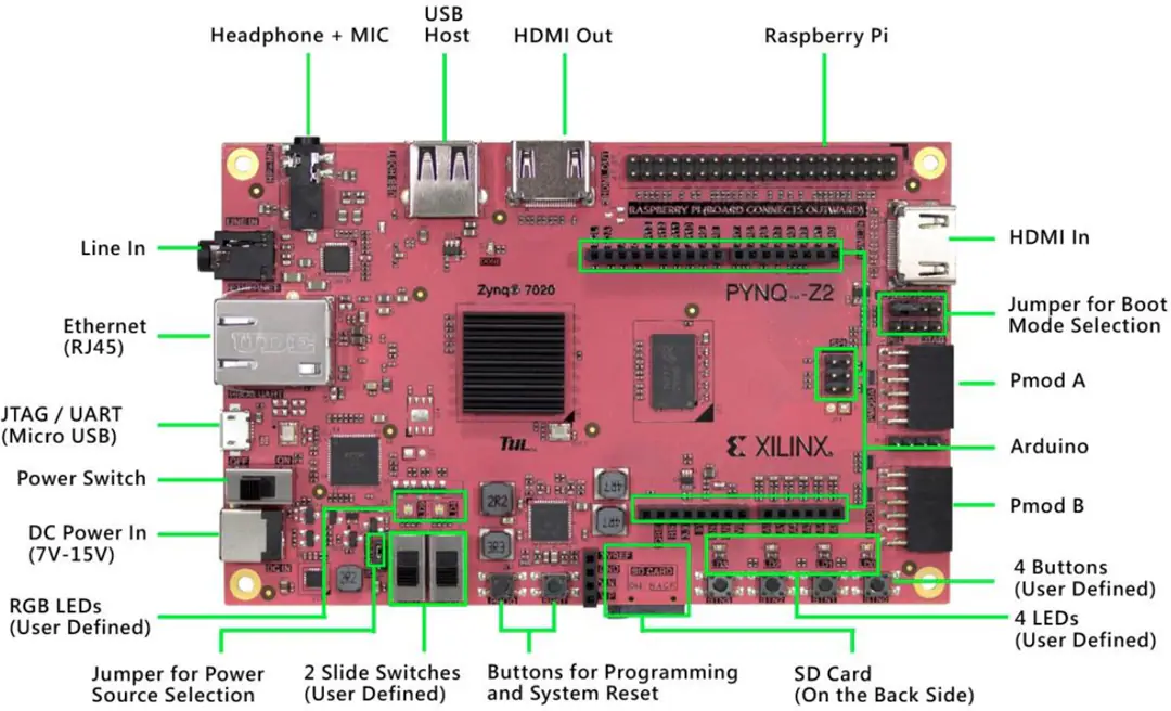
The wrapper derives a 50 MHz internal clock from the board reference and exposes status signals through LEDs and Pmod pins.
Simulation and implementation
The verification set covers individual cores, the AXI transaction path, firmware-driven SoC behavior, and post-route implementation evidence.
AXI4-Lite handshakes and register-visible completion are exercised before comparing the algorithm outputs.
Dedicated AES, SHA-256, and ChaCha20 benches check the expected result and single-start behavior.
Post-route evidence records 0 DRC warnings, 0 ns TNS, and a positive 2.840 ns WNS at the target clock.
CPU-only vs CPU + coprocessor
The same three workloads are executed by PicoRV32 firmware alone and by the memory-mapped accelerator design.
Across AES-like, SHA-like, and ChaCha-like workloads, the coprocessor path reduces the combined measurement from 5,211 cycles to 1,853 cycles.
| Workload | CPU-only | Accelerated | Gain |
|---|---|---|---|
| AES-like | 1,196 | 367 | 3.26× |
| SHA-like | 2,608 | 529 | 4.93× |
| ChaCha-like | 1,244 | 794 | 1.57× |
| Total | 5,211 | 1,853 | 2.81× |
The SHA-like workload shows the largest speedup because its round schedule benefits most from dedicated state and constant storage.
Project demo / video evidence
The demo video shows the recorded execution evidence for the PYNQ-Z2 implementation, including the software-to-coprocessor handshake and visible status behavior.
Watch demo video ↗The engineering decision
The coprocessor spends fabric, memory, timing margin, and power to remove expensive software round loops. The point is not zero cost; the point is a better system-level balance.
Dedicated round logic grows from 958 to 9,132 Slice LUTs, while Slice Registers increase from 662 to 8,092 (+1,122.4%). The accelerated SoC still uses only 17.17% of the available LUTs and 7.61% of the available registers.
Why accept it: crypto rounds repeat predictably and are a better fit for parallel combinational logic than long firmware loops.BRAM rises from 2.5 to 11.5 tiles because the SoC now stores shared buffers and accelerator state.
Why accept it: the memory cost buys a clean MMIO contract and keeps input/result movement deterministic.WNS margin is reduced, but the post-route result remains positive, so the 50 MHz target still passes timing.
Why accept it: the clock margin is spent on useful datapath work, not on an unresolved timing violation.Estimated on-chip power increases by 18.1% as additional crypto logic and memory become active.
Why accept it: the increase is bounded while workload time falls from 5,211 to 1,853 cycles.The accelerated path turns the added hardware into a measurable system benefit: 3.26× for AES-like work, 4.93× for SHA-like work, and 1.57× for ChaCha-like work. It also uses 0 DSPs, keeps slice utilization at 22.47%, and closes timing with positive slack.
The takeaway
CryptoCore RV32 keeps the RISC-V software model simple while moving the expensive, repetitive rounds into purpose-built hardware. The result is a compact SoC that is measurable at the firmware boundary and explainable at the RTL boundary.
Back to top ↑